



Samsung Starts Developing Custom HBM for Meta's AI Chips
Samsung Electronics has started developing custom high-bandwidth memory (HBM) for Meta's in-house AI chips. The article mentions the base die of HBM4E, a seventh-generation HBM.
បច្ចេកវិទ្យា
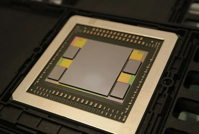
C. Spille/pcgameshardware.de · ដើម · CC BY-SA 4.0 Resized and cropped for display.
AI 반도체 곁에서 데이터를 빠르게 공급하는 적층 메모리예요.
AI 반도체의 성능과 생산·공급망을 함께 이해하는 단서예요.
SK hynix — HBMអានសព្វវចនាធិប្បាយSamsung Electronics has started developing custom high-bandwidth memory (HBM) for Meta's in-house AI chips. The article mentions the base die of HBM4E, a seventh-generation HBM.
Samsung Electronics is developing custom high-bandwidth memory (HBM) for Meta's next-generation in-house AI chip. The base die of the seventh-generation HBM4E will be made at Samsung's 2-nanometer foundry.
A UC Riverside research team published a technical paper on where to place control functions for HBM4 high-bandwidth memory, either on the processor side or the memory base chip. HBM4 allows the bottom chip of the memory stack to hold more complex logic, which makes this placement study possible.
Samsung Electronics is reportedly strengthening its chip packaging business in Onyang, South Korea, to boost both its HBM and foundry competitiveness.
Google unveiled the security-focused TPU '8tx' and the long-context TPU '8i Max', bringing its 8th-generation TPU lineup to four models. TPUs are AI chips Google designs. The high-bandwidth memory (HBM, fast memory attached to chips) that goes with each chip also varies by use.
A report says TSMC, the world's largest contract chipmaker, is considering increasing production of advanced memory for AI chips. Reuters reported this, citing the IT outlet The Information. Since it is still at the review stage, it is unclear whether it will lead to actual investment or mass production.
Nvidia has reportedly asked TSMC, the world's largest contract chipmaker, to produce next-generation 3D DRAM. As the prices of high-bandwidth memory (HBM, memory that stacks multiple layers of DRAM to move data quickly) rise and supply runs short, the move appears aimed at reducing Nvidia's reliance on existing memory makers.
This week, the biggest chip industry news was that Nvidia's board has started an internal review of CEO Jensen Huang. Reports also revealed routes used to smuggle AI chips and high-bandwidth memory (HBM) to China. There was also news that Micron has halted construction of a plant in Taiwan and that Samsung plans to expand HBM production.
In data centers that run AI services, how usefully companies use high-bandwidth memory (HBM, fast memory attached next to the GPU) has become important, because it is fast but expensive and scarce. NVIDIA says it is solving this problem by designing chips, software, CPUs, and storage together.
Samsung Electronics plans to produce base dies, the bottom chips of HBM (high-performance memory made by stacking several DRAM chips), at its Taylor Fab 2 in Texas. The goal is to supply customers such as AMD. However, analysts say Samsung could lose its leading position in the domestic industry if Nvidia has its base dies made by TSMC.
As Samsung Electronics and SK hynix expand investment in high-bandwidth memory (HBM, a high-performance memory that stacks layers to move data quickly) and advanced DRAM, the local workforce of chip equipment companies has also grown sharply. The three companies ASML, Lam Research, and Tokyo Electron have a combined 7,800 employees in Korea this year.